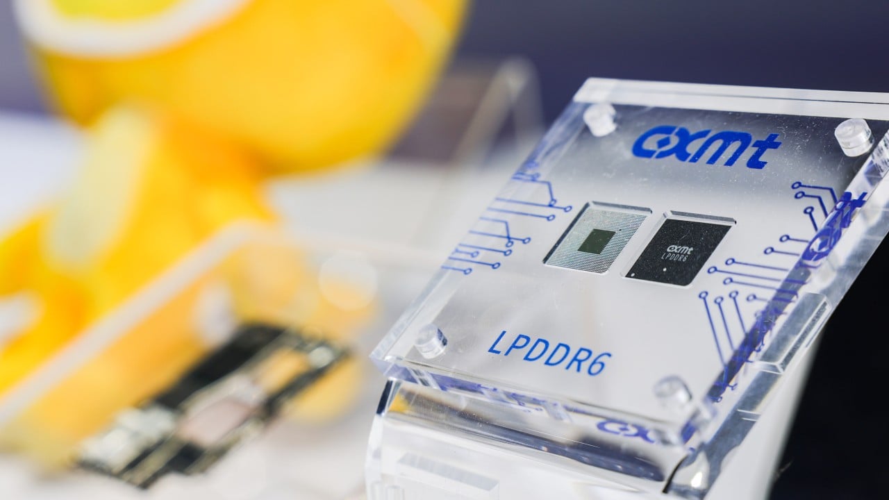
The physical scaling limits of dynamic random-access memory have transformed architectural layout choices from routine process refinements into fundamental survival parameters. As memory half-pitches press past the 11-nanometre threshold, traditional planar transistor structures face diminishing returns, governed by quantum leakage and severe area constraints. Within this trajectory, ChangXin Memory Technologies has introduced engineering developments targeting the 4F2 memory cell architecture—a structural pivot long pursued by industry leaders Samsung Electronics and SK Hynix.
Deconstructing this transition requires analyzing the geometric, electrical, and manufacturing realities that separate conceptual layout designs from viable enterprise-grade production. For a deeper dive into this area, we suggest: this related article.
The Geometric Imperative: Moving from 6F2 to 4F2
In conventional dynamic random-access memory design, the standard memory cell occupies an area of 6F2, where F represents the minimum feature size or half-pitch. This layout couples a planar access transistor with a storage capacitor placed adjacent to or slightly offset from the active area. While this configuration has sustained memory scaling for decades, it hits a hard geometric barrier as lithographic scaling slows down.
The transition to a 4F2 cell architecture compresses the footprint of each individual bit by rearranging the access transistor and placing it vertically. By stacking components rather than spreading them across a horizontal plane, the theoretical cell area shrinks by one-third for an identical feature size. For further information on the matter, extensive analysis can also be found on Ars Technica.
Conventional 6F2 Layout:
[ Capacitor ] -- [ Planar Transistor ] (Horizontal Area: Large)

Proposed 4F2 Vertical Layout:
[ Vertical Transistor (VSG) ]
       |
[ Stacked Capacitor ] (Vertical Footprint: Minimized Area)
This layout multiplication directly alters the density equation. Fitting fifty percent more cells into an equivalent silicon array area bypasses the immediate need for extreme sub-10nm lithographic shrinkage, shifting the engineering challenge from photolithography to vertical integration.
The Electrical Bottleneck: Managing Vertical Surrounding Gate Leakage
Compressing cell area introduces severe electrical penalties. As transistors scale down vertically, channel lengths shorten, exponentially increasing subthreshold leakage current. When a memory cell cannot effectively isolate its stored charge, data retention times drop below acceptable thresholds, rendering the chip unstable.
To combat this, structural designs rely on architectures such as the Vertical Surrounding Gate (VSG) transistor. Unlike planar variants where the gate controls the channel from a single side, a surrounding gate wraps entirely around the vertical channel.
The mechanism relies on three distinct physical advantages:
- Gate-All-Around Control: Electrostatic control is exerted from multiple directions, choking off parasitic leakage paths even as gate lengths shrink.
- Reduced Drain-Induced Barrier Lowering: Enhanced channel grip prevents the drain voltage from prematurely lowering the potential barrier, maintaining high off-state resistance.
- Optimized Aspect Ratio Management: High-aspect-ratio structures—such as capacitor arrays reaching ratios of 45:1 paired with advanced high-k metal gate (HKMG) processes—attempt to keep core cell heights manageable (such as sub-7,000 nm heights) while preserving storage capacitance.
However, these electrical fixes create secondary manufacturing friction. Integrating high-k metal gates into a dense vertical DRAM process flow requires redesigning etch, deposition, and planarization steps that were originally optimized for planar architectures.
The Thermal and Reliability Constraints of Server-Grade Integration
Consumer-grade density claims frequently collapse when confronted with enterprise server environments. High-performance computing nodes demand continuous operation under extreme thermal loads, strict power envelopes, and zero tolerance for soft errors caused by alpha particles or cosmic rays.
When memory density increases by fifty percent per unit area, thermal dissipation density rises proportionally. Heat concentrated within tightly packed vertical pillars accelerates dielectric wear and increases leakage currents, creating a positive feedback loop of thermal degradation.
Furthermore, enterprise validation requires absolute timing synchronization across multi-channel interfaces like DDR5 and LPDDR5X, alongside strict command-address integrity. A dense memory array that achieves high yields in a laboratory setting often fails when subjected to the multi-vendor motherboard compatibility testing required by major hyperscalers. Yield rates for complex architectures frequently hover between twenty and thirty percent during initial transition phases, making unit economics unviable until defect densities are systematically engineered out of the fabrication line.
Strategic Outlook
The race toward 4F2 architectures by major memory producers is not merely an academic exercise in miniaturization; it is an economic necessity dictated by the limits of extreme ultraviolet lithography cost scaling. While announcements of engineering sample completions and roadmap alignments by Samsung, SK Hynix, and CXMT signal an industry-wide convergence on vertical channel transistors, the operational chasm between sampling and high-volume manufacturing remains wide.
The competitive outcome will be determined entirely by manufacturing execution—specifically, which entity can stabilize vertical gate profiles, solve high-aspect-ratio capacitor collapse, and scale enterprise yields past the threshold of commercial viability.