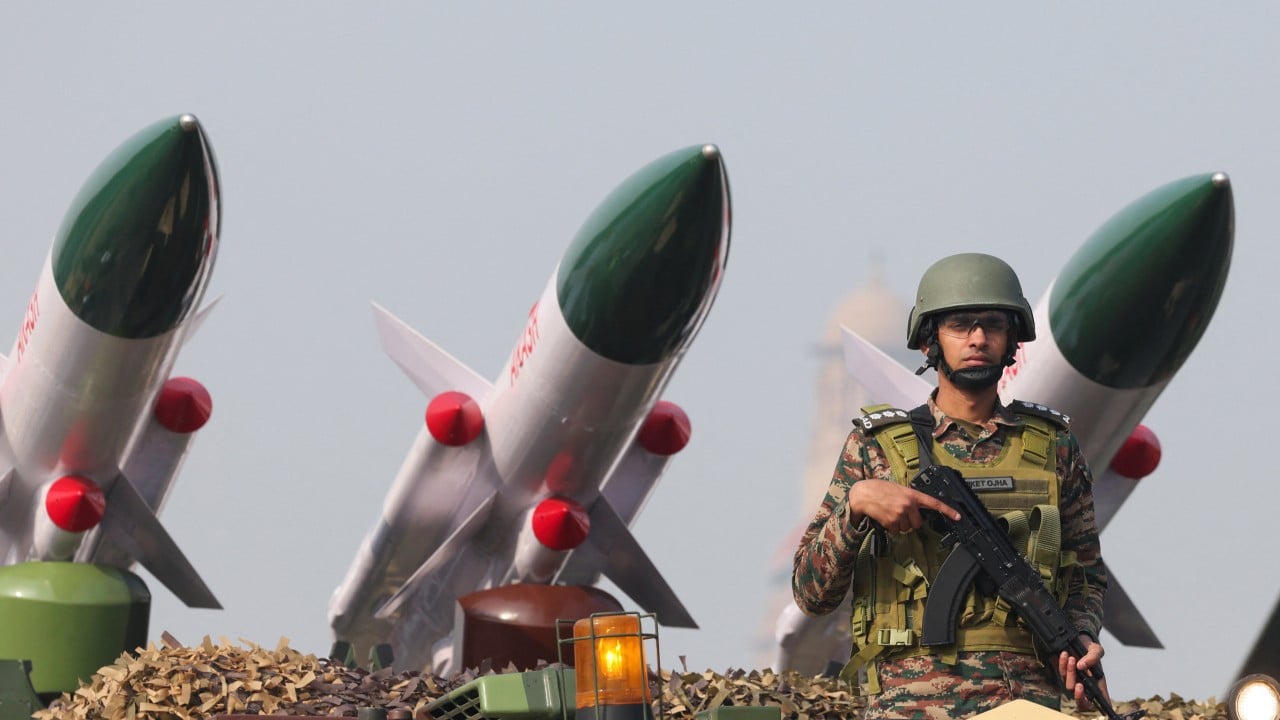
The containment architecture of the global semiconductor supply chain relies on a single, binary assumption: that preventing the physical delivery of an ASML Extreme Ultraviolet (EUV) lithography system to mainland China permanently freezes Beijing’s native advanced logic capabilities. This assumption underpins the current frictions between the United States Department of Commerce and ASML senior leadership regarding allegations that an EUV system, or its highly specialized transport infrastructure, bypassed export controls.
The focus on tracking a single 180-ton machine misses the structural physics of semiconductor manufacturing. To understand why a single transrouted or diverted EUV system cannot alter the geopolitical equilibrium, one must evaluate advanced semiconductor fabrication not as a collection of hardware assets, but as an operational cost function dependent on continuous, closed-loop supply chains. An isolated EUV machine operating in a vacuum decays rapidly into a non-functioning multi-million-dollar monument.
The Dislocation of Capital and the Structural Realities of Lithography
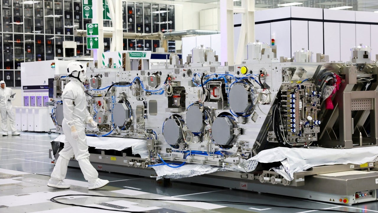
To evaluate the validity and impact of an EUV security breach, the system must be disassembled into its core dependencies. An ASML Twinscan EUV system requires a continuous, high-volume operational infrastructure that cannot be faked or sustained through domestic substitution in the short term. The machine is defined by three absolute pillars of dependency.
The Upstream Component Bottleneck
An EUV scanner is comprised of more than 100,000 discrete subsystems sourced from a highly integrated, Western-aligned supplier matrix. The optical train, engineered by Carl Zeiss in Germany, uses sub-nanometer-smooth mirrors to direct 13.5-nanometer wavelength light. The laser-produced plasma (LPP) light source, engineered by Cymer in the United States, generates this light by striking 50,000 falling droplets of molten tin per second with a high-power carbon dioxide laser.
If any single sub-component in this optical or excitation path degrades—a mathematical certainty given the extreme thermal and kinetic stresses within the vacuum chamber—the system halts. A diverted machine lacks access to the automated, authenticated telemetry networks and spare parts pipelines required to maintain uptime.
The Yield and Consumables Function
Lithography does not occur in isolation. The exposure tool must interface perfectly with the track system that applies and develops advanced photoresists, such as chemically amplified resists (CAR) or newer metal oxide resists (MOR). These specialized chemical formulations are dominated by Japanese suppliers like Tokyo Ohka Kogyo and JSR Corporation. Without access to these precise chemical specifications, a smuggled EUV tool experiences severe line-edge roughness and critical dimension defects, rendering the output wafer yield economically unviable.
The Operational Field Engineering Deficit
ASML maintains a worldwide fleet of over 300 operational EUV systems by deploying dedicated, specialized field applications engineers who reside permanently at customer fabrication plants (fabs). These engineers manage real-time machine calibration, sub-lens aberration corrections, and regular preventive maintenance overhauls.
Because ASML walls off its China-based personnel from EUV documentation, training, and software patches, a domestic engineering team attempting to maintain a smuggled scanner faces an insurmountable learning curve. The software architecture alone, which handles precise alignment at the picometer scale between the wafer stage and the reticle stage, requires continuous diagnostic feedback loops connected directly to ASML's central data repositories in Veldhoven.
The Alternative Path: DUV Multipatterning Costs
The true friction in the Chinese semiconductor industry is not the presence or absence of a single EUV machine, but the economic calculation of running advanced nodes on older Deep Ultraviolet (DUV) immersion equipment. China’s largest foundry, Semiconductor Manufacturing International Corporation (SMIC), has successfully demonstrated the production of 7-nanometer and 5-nanometer class features using ASML’s Twinscan NXT:2000 series DUV immersion systems.
To achieve these features without 13.5nm EUV light, fabs must use Self-Aligned Quadruple Patterning (SAQP). The process decomposes a single circuit layer into four separate lithography exposures, four distinct photoresist bakes, and multiple subsequent etching and deposition cycles.
This multi-step approach drastically alters the total cost structure per wafer through two primary mechanisms:
- The Yield Decay Multiplier: If a single lithography step features a 90% yield, a single-exposure EUV layer retains a 90% yield. An SAQP process requiring four successive exposures compounded by etching steps reduces the effective layer yield exponentially ($0.90^4 \approx 65.6%$). In practice, reports indicate SMIC’s advanced DUV patterning nodes operate at yields below 50%.
- The Throughput Chokepoint: Running a wafer through a DUV immersion tool four times to print one layer consumes four times the machine hours. This creates a severe bottleneck, reducing the total wafer-per-hour output of the fab and escalating capital depreciation costs per chip.
The Chinese state covers these operational losses via direct capital injections and domestic subsidies, keeping entities like Huawei supplied with native silicon. This model works for low-volume strategic applications, such as domestic artificial intelligence accelerators and infrastructure hardware. However, it cannot scale to match the consumer electronics cost curve or high-volume global markets commanded by competitors using optimized EUV processes.
The Timeline for Domestic EUV Replicability
Because smuggling complete systems cannot provide industrial-scale capacity, the Chinese state has focused its long-term strategy on domestic development. This program operates via a parallel track completely separate from the Western supply chain, aiming to deliver a fully domestic EUV system by approximately 2030 to 2035.
A domestic system cannot simply copy ASML's design because the component supply chain remains blocked by export controls. Instead, Chinese research institutes, under the coordination of the state, are pursuing alternative physics architectures:
[Domestic Research Consortium]
       │
       ├── Light Source: Laser-Induced Discharge Plasma (LDP) / Synchrotron SSMB
       ├── Optics: Shanghai Institute of Optics and Fine Mechanics (SIOM)
       └── Stage Metrology: Precision Interferometer Systems
Instead of using Cymer’s Laser-Produced Plasma (LPP) architecture, domestic prototypes are evaluating Laser-Induced Discharge Plasma (LDP) and large-scale synchrotron radiation facilities using Steady-State Microbunching (SSMB). SSMB provides a high-power, highly stable EUV light source, but it requires building a particle accelerator directly attached to the fabrication plant. This is a radical departure from ASML’s modular, self-contained fab footprint.
The primary obstacle for this native track is the manufacturing of the reflective optics. Western systems use mirrors polished to an accuracy of less than 0.1 nanometers, achieved through ion beam milling and precise surface metrology.
While the fundamental physics of this polishing process are thoroughly documented in public academic literature, reproducing the machinery that performs this polishing at scale remains a severe engineering bottleneck. Domestic entities like the Shanghai Institute of Optics and Fine Mechanics face decades of iterative optimization to transition from producing a single laboratory-grade reflective surface to manufacturing resilient optics that withstand constant EUV radiation without degrading.
Strategic Outlook and Market Consequences
The introduction of legislative measures like the MATCH Act in the United States highlights a shift toward a total embargo on advanced lithography servicing. If expanded to prohibit the maintenance and spare parts supply for the massive installed base of DUV immersion tools already operating inside China, the containment strategy will shift from an expansion prevention model to an active degradation model.
Under an active degradation framework, the operational capacity of Chinese foundries will contract over a rolling 24-to-36-month window as existing DUV tools consume their operational spares, experience laser source degradation, and exhaust their optical alignment tolerances. This will force a stark bifurcation in the global technology sector.
Western chip manufacturers will continue up the scaling curve toward Sub-2nm nodes using High-NA (0.55 NA) EUV tools, while Chinese foundries will be forced to allocate substantial engineering resources to reverse-engineer basic maintenance components for older DUV tools just to maintain current output levels.
The ultimate baseline for the global semiconductor market is clear: the technological chokepoint is not a physical asset that can be illicitly moved across a border. It is an ongoing, highly collaborative, multi-national industrial process.
For corporate strategists and sovereign policymakers, the critical metric to track is not the rumor of an isolated container moving into a Chinese port, but rather the operational yield metrics of domestic Chinese DUV multi-patterning lines and the power-output milestones of their alternative synchrotron light sources. Those are the real metrics that dictate when, and if, the current technological containment line will shift.