The tech press is throwing another victory party for a technology that cannot survive outside a cleanroom.
Every few months, a headline emerges claiming that a corporate titan or a state-backed research institute has built a new 2D parallel computing chip that "rewrites Moore’s Law." The narrative is incredibly predictable. Silicon is tired. Silicon is hitting its atomic limits. Therefore, atomic-thin sheets of transition metal dichalcogenides (TMDs) like molybdenum disulfide ($\text{MoS}_2$) or tungsten diselenide ($\text{WSe}_2$) will step in, enable massive parallel architectures, and keep the exponential growth of computing power alive forever.
It is a beautiful story. It is also completely detached from the brutal realities of semiconductor manufacturing.
The hype machine treats the fabrication of a few dozen working transistors on a microscopic flake of 2D material as a historic breakthrough. It is not. It is an expensive science project. The industry does not need another laboratory miracle; it needs billions of identical, defect-free features produced at a yield rate exceeding 90% on a twelve-inch wafer. 2D materials cannot deliver this, and pretending they will soon replace or fundamentally rewrite the trajectory of silicon is actively misleading.
The Flawed Premise of Parallel 2D Overhaul
The core argument driving this recent excitement rests on a fundamental misunderstanding of what actually stalls chip performance today. Cheerleaders argue that by stacking atomic-thin 2D materials into parallel computing channels, we can bypass the short-channel effects that plague sub-2-nanometer silicon. Because 2D materials are ultra-thin, the gate electrode can maintain perfect electrostatic control over the channel, preventing current leakage even at minuscule dimensions.
This is technically true in a vacuum. In practice, it ignores the law of parasitic resistance.
When you scale a material down to a single atomic layer, you drastically reduce the cross-sectional area through which electrons can flow. Basic physics dictates that a smaller cross-sectional area increases electrical resistance. To hook these 2D layers up to the rest of the chip, you must form metal-semiconductor junctions. At the atomic scale, the contact resistance between the metal lines and the 2D material skyrockets.
I have watched hardware teams torch millions of dollars trying to optimize contact engineering on novel substrates. You can design the most elegant parallel architecture on paper, but if your electrons are choking at the front door because the contact resistance is too high, your revolutionary chip runs slower than a ten-year-old silicon node. The "parallel" aspect is not a brilliant shortcut; it is a desperate attempt to compensate for the fact that a single 2D channel cannot carry enough current to drive a modern clock speed.
The Yield Crisis Nobody Wants to Discuss
Let's address the elephant in the fab: synthesized 2D films are structurally miserable.
Silicon is a mature marvel because we can grow massive, single-crystal ingots with virtually zero dislocations. You can slice it, polish it, and print billions of features with atomic precision. 2D materials, typically grown via Chemical Vapor Deposition (CVD), are polycrystalline. They are collections of tiny crystalline grains that smash into each other, creating grain boundaries.
Think of grain boundaries as microscopic roadblocks. Every time an electron hits one, it scatters, generating heat and slowing down. More importantly, these defects are random. In a mass-manufacturing environment, randomness is fatal. If Transistor A crosses three grain boundaries and Transistor B crosses none, their electrical characteristics will be wildly different.
Silicon:      [---Uniform Single Crystal Substrate---] -> Predictable Performance
2D Materials: [Grain A] | [Grain B] | [Grain C]       -> Random Electron Scattering
                        ^           ^
                 Grain Boundaries (Defects)
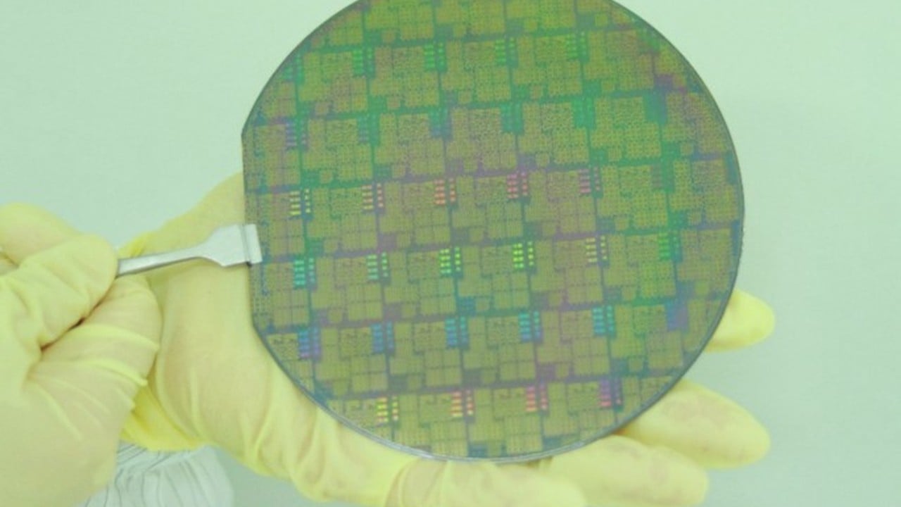
A modern processor requires billions of transistors to behave exactly the same way at the exact same voltage. A deviation of even a few millivolts across a die ruins the entire wafer. When researchers brag about a "parallel 2D computing chip," they are quietly filtering out the failed devices. They choose the one pristine area of the substrate that worked, run their tests, write their paper, and ignore the sea of dead transistors surrounding it. That is acceptable for an academic journal. It is a commercial fantasy.
The Interconnect Nightmare
Even if a manufacturer miraculously solves the yield and resistance issues, they run headfirst into the physical wall of backend-of-line (BEOL) interconnects.
Making transistors smaller or splitting them into parallel 2D planes does not solve the data routing problem. The true bottleneck in modern computing isn't the speed of the switch; it is the time and energy it takes to move data from the memory to the logic units. Copper wires at the sub-10nm scale suffer from massive resistivity increases due to electron scattering at the wire surfaces and grain boundaries.
Stacking 2D materials to create parallel logic channels sounds great until you realize you now need to route vertical vias through those layers to connect them. The aspect ratio of these vias becomes absurdly tight. You are trying to drill and fill holes that are nanometers wide through multiple dissimilar materials without causing delamination, thermal mismatch cracks, or electrical shorts.
The industry is already struggling to handle thermal dissipation in standard 3D silicon packaging. Stacking highly resistive 2D layers on top of each other creates a localized thermal trap. Without a revolutionary breakthrough in thermal interface materials, a dense, parallel 2D chip would instantly bake itself to death under a standard workload.
Dismantling the Frequently Asked Questions
The public discourse around this technology is warped by hype. To see the reality, we have to look directly at the common assertions and break down why they are flawed.
Can 2D materials extend Moore's Law?
No. The assumption that Moore's Law is merely a statement about physical dimensions is wrong. Moore’s Law is an economic rule disguised as a physics principle. It states that the number of transistors on a microchip doubles roughly every two years while the cost of computers is halved.
Even if 2D materials allow for smaller physical features, the lithography, deposition, metrology, and yield-learning curves associated with exotic materials like $\text{MoS}_2$ are exponentially more expensive than staying on silicon variants. If a chip layout costs ten times more to produce for a mere 20% gain in power efficiency, Moore’s Law is dead, regardless of how thin the channel is.
Why are major firms investing heavily in this research if it is a dead end?
It is a hedge, not a product roadmap. Major players invest in high-risk, exotic material research for defensive intellectual property reasons and state-funded grant compliance. They need to own the patents just in case a competitor stumbles upon an unexpected manufacturing breakthrough. But if you look at where their capital expenditure actually goes, it is channeled into EUV lithography optimization, backside power delivery networks (BSPDN), and high-bandwidth memory integration on silicon. They talk about 2D materials in press releases to signal innovation to investors, but they build their revenue on silicon.
Isn't parallel architecture the natural solution to silicon's physical limits?
Parallelism works at the macro architecture level (more cores, specialized accelerators like GPUs and TPUs), but forcing parallelism down into the atomic material layer of the transistor channel creates an unmanageable matrix of parasitic capacitance. When you run multiple 2D channels in parallel to boost current drive, you increase the surface area between the channels and the gates. This introduces parasitic capacitance, which slows down the switching speed of the transistor. You are effectively fixing a current problem by creating a speed problem.
The Hard Truth of Future Computing
The path forward for high-performance computing is not a radical leap to exotic 2D materials. The immediate future belongs to advanced packaging, architecture optimization, and silicon maximization.
Instead of trying to force unreliable atomic sheets into a fabrication process designed for silicon, the industry is winning by ripping up the monolithic chip design entirely. Chiplets, silicon interposers, and co-packaged optics are where the real performance gains are happening. We are learning to build smarter, heterogeneous systems out of known, reliable components rather than praying for a single material savior.
Admitting this requires dropping the romantic notion of a clean break from silicon. It requires acknowledging that the next decade of progress will be an unglamorous war of inches fought over packaging tolerances, power delivery efficiency, and compiler optimization.
Stop waiting for atomic-thin sheets to rewrite the rules of physics and economics. The 2D parallel computing revolution is a mirage that looks perfect from a distance but vanishes the moment you try to scale it.